1 Introduction
Driven by the global emphasis on renewable energy and energy conservation, new energy has experienced rapid development in recent years. The application of voltage source converters (VSCs) utilizing IGBT devices has also become increasingly widespread. To ensure the normal operation of converter equipment, arm shoot-through must always be avoided. Arm shoot-through causes unnecessary additional losses in IGBT devices and can even trigger thermal runaway, potentially leading to the failure of the IGBT modules or even the entire inverter system. Arm shoot-through can occur in both two-level and multi-level topologies. Therefore, this article focuses on the two-level topology to explain the causes of arm shoot-through and the impact of dead time on its occurrence.
1.1 Arm Shoot-through and “Dead Time”
The figure below shows a typical three-phase half-bridge topology. During normal operation, the two IGBTs in each phase leg switch on and off alternately. When both IGBTs in a phase leg conduct simultaneously switch on, a phenomenon known as “arm shoot-through”, the phase current experiences a sharp rise. The rate of this current rise is limited only by the DC bus voltage and the stray inductance in the loop.
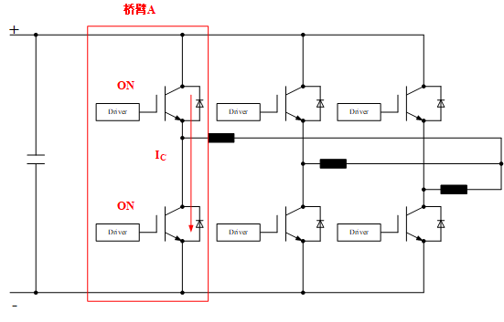
Figure 1: Three-Phase Half-Bridge Topology Diagram
Of course,converters are not designed to turn on both IGBTs simultaneously. However, due to the non-ideal switching characteristics of IGBTs, differences exist in their turn-on and turn-off times, which may lead to arm shoot-through. To prevent shoot-through, it is standard practice to incorporate “dead time” into the control algorithm. During this intentional delay, one IGBT is always turned off first, while the other is only turned on after the dead time expires. This prevents shoot-through caused by asymmetrical IGBT switching times.
1.2 Impact of Dead Time on Converter Operation
While dead time effectively prevents arm shoot-through, it also introduces drawbacks
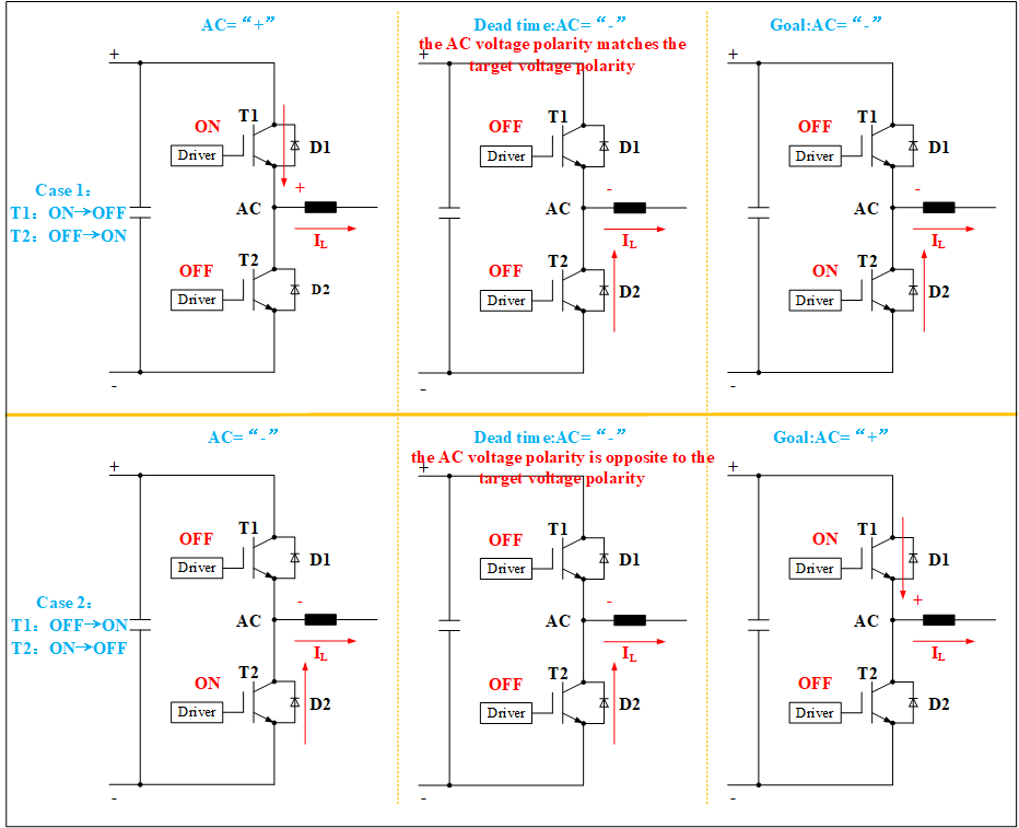
Figure 2: Schematic Diagram of Output Current Direction Impact on AC Output Voltage
As shown in Figure 2, first assume the output current flows in the indicated direction.
Case 1: T1 switches from on to off, and after a short dead time, T2 switches from off to on.During the effective dead time, both switches are off,and the freewheeling diode D2 conducts the output current. At this time, a negative DC voltage is applied to the AC output terminal. When T2 is fully turned on, the AC output ultimately delivers negative DC voltage through T2. Therefore, during the dead time, the AC voltage polarity matches the target voltage polarity, which complies with the design requirements.
Case 2: T1 switches from off to on, while T2 switches from on to off.
At this time, since the current still flows in the same direction, this current continues during the dead time. Thus, the AC output voltage remains negative. However, ultimately the AC output delivers positive DC voltage through T1. Therefore, during the dead time, the AC voltage polarity is opposite to the target voltage polarity, which does not comply with the design requirements.
The conclusion can be summarized as follows: During the effective dead time, the AC output voltage is determined by the output current direction, not by the control signal.
If we assume the output current direction is opposite to that shown in Figure 2, then when T1 switches from on to off while T2 switches from off to on, a similar situation to the above will also occur.Therefore, under normal circumstances, the introduction of dead time will cause distortion in both the system's output voltage and output current.If we select an excessively large dead time, the system will become unstable.Consequently, dead time must be carefully calculated to achieve optimal performance.
2 Selecting Appropriate Dead Time
As discussed, the selection of dead time must satisfy the requirement of preventing arm shoot-through on one hand, while being minimized as much as possible to ensure the proper operation of the converter on the other. Therefore, the major challenge here lies in determining the appropriate dead time for specific IGBT devices and their drivers.
2.1 Dead Time Calculation Formula
We adopt the following formula to calculate dead time, which is Infineon's empirical formula for dead time calculation:

tdoff_max : Maximum turn-off delay time;
tdon_min : Minimum turn-on delay time;
tpdd_max : Maximum driver propagation delay;
tpdd_min : Minimum driver propagation delay;
1.2 : Safety factor (For IGBTs rated 3300V and above, this factor is often increased to 1.5);
In this equation:The first term (tdoff_max–tdon_min)represents the difference between the maximum turn-off delay time and minimum turn-on delay time. This value is most critical at smaller collector currents. This term describes the switching characteristics of the IGBT device itself plus the gate resistor used. Since the fall time and rise time are far smaller than the delay time, they are not considered here.
The second term (tpdd_max–tpdd_min)represents the propagation delay difference of the driver. This parameter is determined by the driver and can be found in the driver datasheet. It generally differs by only hundreds of nanoseconds, but this difference is larger for optocoupler-based drivers.
Since the actual applied bus voltage and collector current in customer applications differ significantly from the test conditions in IGBT datasheets, dead time cannot be accurately calculated by referring to IGBT datasheets. A series of double-pulse tests under specific driving conditions are required to obtain accurate delay times and thereby calculate the dead time.
2.2 Definition of Turn-on/Turn-off Delay Times
We define the switching times of IGBTs in accordance with 《IEC 60747-9-2007 Semiconductor devices – Discrete devices – Part 9: Insulated-gate bipolar transistors (IGBTs)》.
tdon : From 10% of VGE to 10% of ICM;
tr : From 10% of ICM to 90% of ICM;
tdoff : From 90% of VGE to 90% of ICM;
tf : From 90% of ICM to 10% of ICM;
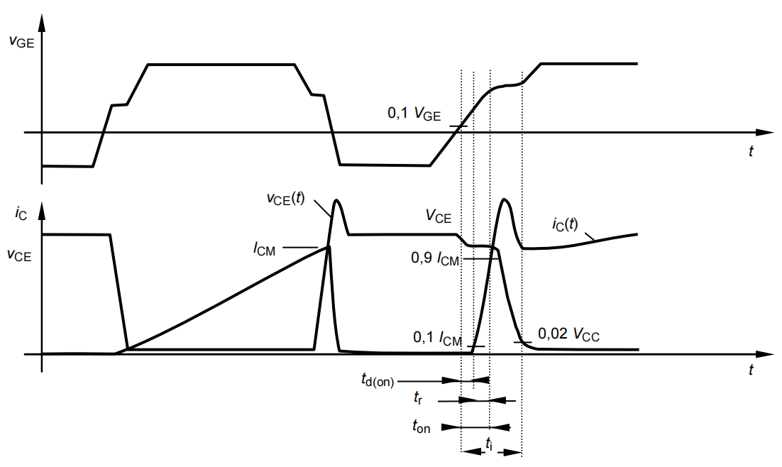
Figure 3: Turn-on Time Definition
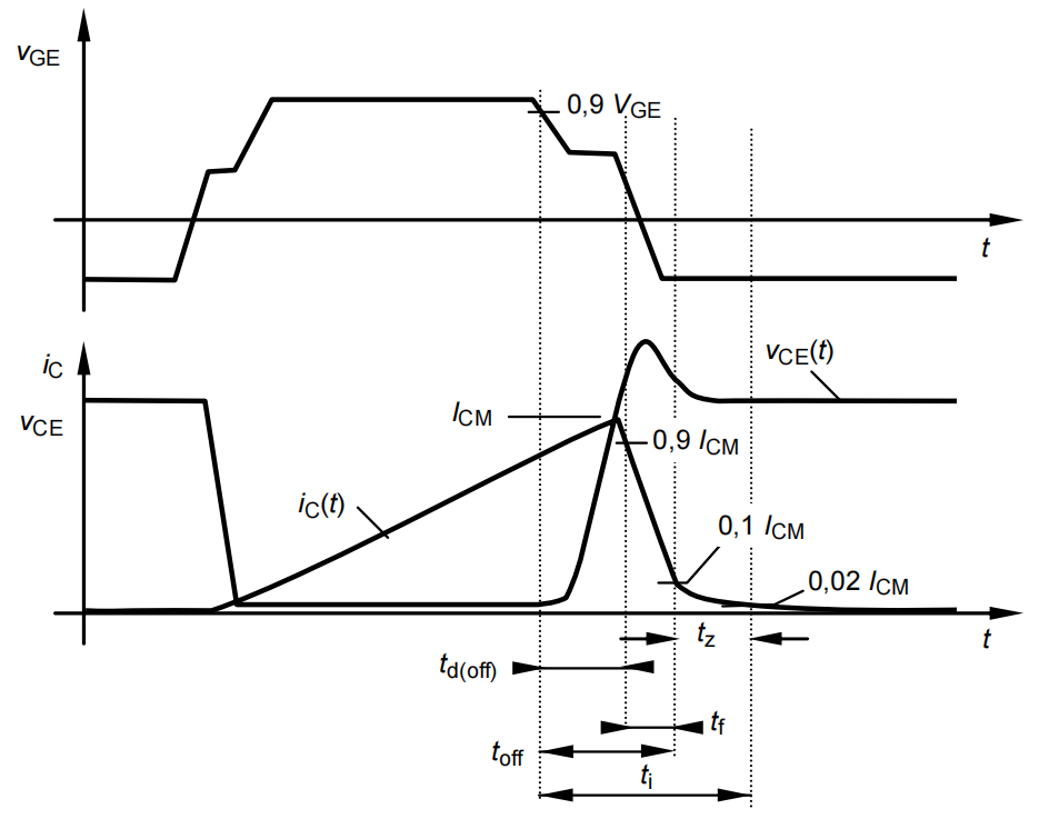
Figure 4: Turn-off Time Definition
2.3 Factors Influencing Turn-on/Turn-off Delay Times
Numerous factors affect the turn-on/turn-off delay times of IGBTs, such as gate resistance, collector current, driver output level, IGBT junction temperature, among others.If the driver is already determined, the primary considerations are gate resistance, IGBT junction temperature, and collector current.
2.3.1 Impact of Gate Resistance on Turn-on/Turn-off Delay Times
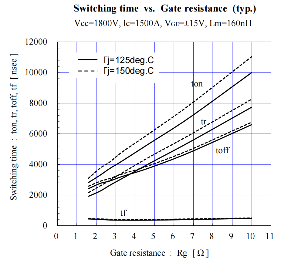
Figure 5: Relationship Diagram Between Turn-on/Turn-off Times and Gate Resistance
As shown in Figure 5 (from Fuji’s 1MBI1500UE-330 datasheet), gate resistance significantly affects IGBT turn-on/turn-off delays.Turn-on and turn-off delays increase as gate resistance increases, necessitating testing under actual gate resistance conditions. The diagram also reveals that IGBT junction temperature impacts delays—higher temperatures result in longer delays. The 1.2 safety factor accounts for junction temperature effects, but for high-voltage modules rated 3300V and above, this coefficient is typically set to 1.5.
2.3.2 Impact of IGBT Collector Current on Turn-on/Turn-off Delay Times
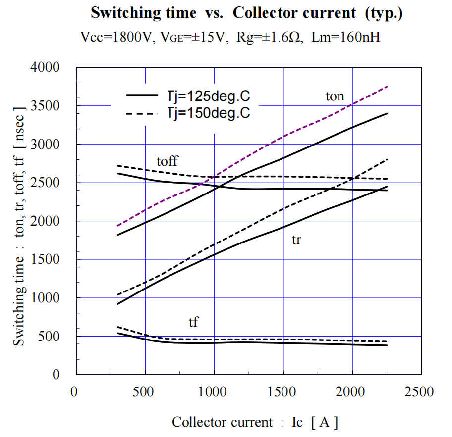
Figure 6: Relationship Diagram Between Turn-on/Turn-off Times and Collector Current
As shown in Figure 6 (from Fuji’s 1MBI1500UE-330 datasheet), we observe that as the collector current decreases, the turn-off delay increases while the turn-on delay decreases. Therefore, under constant bus voltage, smaller collector currents impose stricter requirements on dead time. Consequently,measuring turn-on/turn-off delays under specific driving conditions and then calculating dead time based on the measured values is a better and more precise method. We typically advise customers that measuring turn-on/turn-off delays at rated bus voltage and 10% of the IGBT's rated collector current suffices to calculate the required dead time.
3 Matching System Dead Time
For high-voltage IGBTs above 3300V, an increase in VCE voltage widens the depletion layer, resulting in prolonged turn-off time. Simultaneously, higher VCE extends the time for channel inversion layer disappearance, further delaying the turn-off process. In mining frequency converter applications, most manufacturers purchase ABB controllers externally, where dead time cannot be freely modified. However, the actual required dead time often exceeds the controller's preset value, creating an urgent need for effective system dead time matching.
According to the dead time calculation formula, effective measures to reduce dead time involve either decreasing turn-off delay or increasing turn-on delay. With drivers already fixed, available measures are limited: we can only reduce turn-off delay by decreasing turn-off gate resistance, while also considering IGBT turn-off voltage peaks. Often, we are forced to accept large dead times, compromising system stability. Below are three methods to reduce dead time (though compromises in losses or other aspects may be required):
3.1 Increasing Turn-on Gate Resistance to Extend Turn-on Delay
Considering IGBT safety requirements (turn-off peaks must remain within the Safe Operating Area), when turn-off delay cannot be further reduced by decreasing turn-off gate resistance, we can adopt the reverse approach: increasing turn-on gate resistance to extend turn-on delay, thereby reducing dead time. However, this method requires that the driver's turn-on/turn-off gate resistors be independent. Otherwise, adjusting the gate resistor to increase turn-on delay will simultaneously increase turn-off delay; such coupling may prevent achieving the desired dead time. Additionally, increasing turn-on gate resistance also raises turn-on losses, necessitating evaluation of whether system losses meet design requirements. This method is only suitable for applications where loss requirements are not stringent and does not improve system stability, thus having limitations.
3.2 Digital Drivers Adding Turn-on Propagation Delay
This method optimizes the first approach: digital drivers can artificially increase the turn-on propagation delay without altering turn-on gate resistance, matching the system or controller's preset dead time. The advantage is that the IGBT's turn-on characteristics remain unchanged, with no increase in turn-on losses. The disadvantage is that the system's dead time burden is shifted to the driver, without improving system stability.
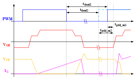
Figure 7: Schematic Diagram of Adding Turn-on Propagation Delay
3.3 Adopting Muti-level Turn-off Technology to Reduce Turn-off Delay
Another approach is Firstack's Muti-level turn-off technology. By switching resistors of different values during distinct stages of IGBT turn-off, this method optimizes the entire turn-off process, achieving reduced turn-off delay while suppressing voltage peaks.
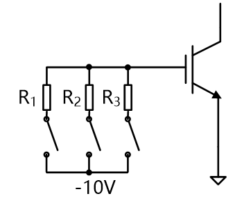
Figure 8: Muti-level Turn-off Schematic Diagram
Figure 9 shows a comparison of turn-off delays for Firstack's HV1027P driver matched with Infineon's FZ1200R45KL3_B5 module under VDC=2000V, IC=100A. As seen in the figure:Without Muti-level turn-off function: Turn-off delay = 8.212μs;With Muti-level turn-off function: Turn-off delay = 6.212μs.The turn-off delay is reduced by nearly 25%, effectively decreasing dead time and improving system stability.
CH1:VGE, CH2:VCE, CH4:IC
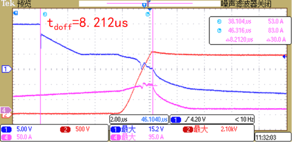
Figure 9a: Without Muti-level turn-off function
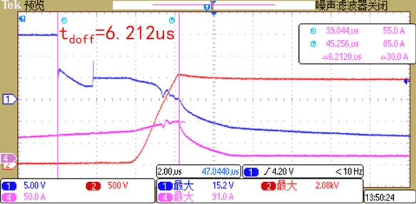
Figure 9b: With Muti-level turn-off function
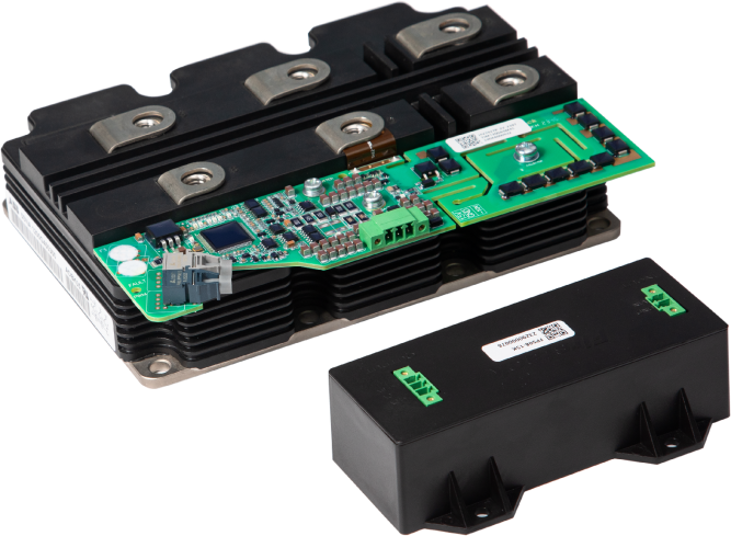
Figure 10: HV1027P Product Schematic Diagram
4 Conclusion
Dead time can effectively prevent arm shoot-through short circuits. However, excessive dead time affects system stability. Meanwhile, gate resistance significantly impacts IGBT turn-on/turn-off delays, and smaller collector currents impose stricter requirements on dead time. Therefore, it is necessary to test turn-on/turn-off delays under specific driving conditions to accurately evaluate dead time.
Additionally, with drivers already fixed, the method of reducing dead time by adjusting gate resistance has significant limitations. Firstack's intelligent drivers can help customers optimize turn-on/turn-off delays through digital delay, muti-level turn-off technology, and other means, thereby effectively matching system dead time and ensuring safe operation of converters.