1.Abstract
The Power Conversion System (PCS) is the core equipment in energy storage systems, primarily responsible for bidirectional power conversion between batteries and the grid. The PCS not only converts DC power to AC power (inversion) but also converts AC power to DC power (rectification) to meet the charging and discharging requirements of the energy storage system (ESS). The performance of the PCS directly impacts the efficiency, stability, and reliability of ESS, making it be a critical component. The Power Module, which performs the actual power conversion, is the core component of the PCS. The following sections will discuss key aspects of power module design, including topology, module selection and key technologies of gate driver.
2.Technology Features
In commercial & industrial (C&I) energy storage, PCS units typically have power ratings of 100kW, 125kW, and 200kW. For utility-scale energy storage (large-scale storage), mainstream PCS units are rated at 1.25MW, 1.75MW, and 2.5MW. The evolution of high-power PCS topologies has been closely tied to battery voltage levels:
1.2015: Maximum battery voltage was 800V, and two-level topology was commonly used.
2.2017: Battery voltage increased to 1200V, leading to the adoption of NPC (Neutral-Point Clamped) three-level topology.
3.2019 onward: With battery voltages reaching 1500V, the ANPC (Active Neutral-Point Clamped) three-level topology became the mainstream solution.
High-power PCS units typically operate at rated charge/discharge currents between 1050A and 2100A. To achieve these power levels, EconoDUAL™ standard modules are combined in ANPC three-level configurations with parallel connections, such as:
· 3-parallel ANPC for 1.25MW
· 4-parallel ANPC for 1.75MW and 2.5MW
The following figure shows the combination form, layout structure and control mode of IGBT module for power above 1.75MW.
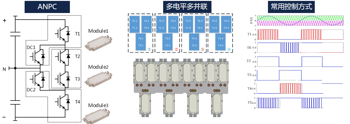
IGBT Combination Topology Control
Fig. 1 Power Stack Design
Key Challenges in PCS Design and Application:
· ANPC Three-Level Timing Protection
· Dead-Time Selection in PCS
· IGBT Short Pulse Issues
· PWM Interference due to EMC Problems
3.Solutions
1). Complete ANPC three-level Timing Protection
The ANPC three-level topology presents critical challenges in the turn-off sequence between inner and outer switches, where the outer switches must be turned off prior to the inner switches. During normal start/stop operations of the PCS, this sequencing is managed by the system controller. However, in cases of power device failures within the PCS, the gate driver must assume control to ensure proper sequential protection.
Firstack's ED-WP-CB series intelligent gate drivers address these requirements by continuously monitoring all PWM input signals and IGBT operating states to execute precise ANPC three-level sequential shutdown. Furthermore, the driver maintains this critical functionality even during non-semiconductor fault conditions such as control signal anomalies or power supply interruptions, autonomously managing the inner and outer switch turn-off sequence to ensure system protection.
This advanced capability provides robust protection against potential failure modes while maintaining system reliability under both normal and fault conditions.
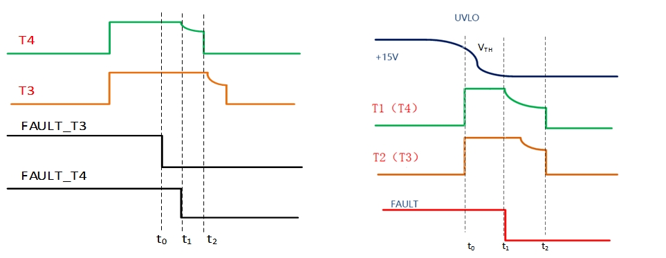
Module Failure Non Module Failure
Fig. 2 Time Protection Logic in 3-level System
2). Dead Time Selection
Dead time refers to a short delay intentionally set between the turn-off and turn-on in a bridge circuit during PWM switching. Its main purpose is to prevent both switches from conducting simultaneously, which could cause dangerous short-circuit conditions. In PCS systems, dead time affects performance in two ways, it reduces the effective battery charging voltage (DC voltage utilization) - longer dead times mean lower charging voltage and impacts power quality by increasing THD (Total Harmonic Distortion) on the AC side.
The dead time for the designed PCS can be determined through double-pulse testing of the power module. The calculation formula for dead time is as follows:
Dtime=[(td_off_max-td_on_min)+(tG_max-tG_min)]*k
td_off_max is the maximum turn off delay time; td_on_min is the minimum turn on delay time; tG_max is the maximum signal transmission delay; tG_min is the minimum signal transmission delay. k is safety constant,normally around 1.2-1.5. Based on extensive testing and understanding of switching characteristics from different IGBT manufacturers worldwide, Firstack recommends a dead time range of 5μs-6μs for optimal PCS operation.
The ED-WP-CB series features built-in 4μs minimum dead time protection. Follows control system's dead time setting when ≥4μs and enforces 4μs minimum when control system requests <4μs. Effectively reduces PCS failure risks associated with improper dead time settings.
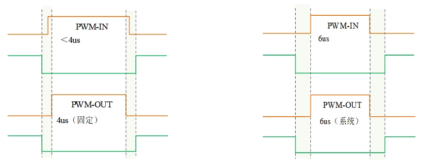
4μs dead time 6μs dead time
Fig. 3 Dead time logic of ED-WP-CB series
As demonstrated above, insufficient dead time can lead to power module failure. To compensate for the reduction in overall DC voltage utilization in energy storage systems, the following control strategies may be incorporated into the control scheme:
Third-Harmonic Injection and Dead-Time Compensation Algorithm.
3). Short Pulse
Turning off an IGBT before it's fully conducting (when carrier concentration is too low) can lead to excessive turn-off voltage spikes, increased switching losses, and gate oxide layer degradation. For unity power factor (PF=1), short pulses occur at current minimums, while at PF=-1 they appear at current peaks. Since high-power PCS modules typically have gate charges (QG) ranging 4-13μC, sufficient conduction time is essential. Based on test data analysis, we recommend maintaining IGBT pulse widths ≥5μs, with control systems filtering out any sub-5μs pulses to ensure reliable operation.
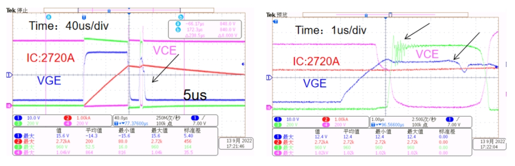
5μs General View Zoom In View
Fig. 4 IGBT Short Pulse Test
As shown in Fig. 4, a double-pulse experimental diagram of 1200V/600A three-level 4-parallel ANPC topology, the second pulse time is 5us, at this time, the VGE voltage can't reach 15V, the diode oscillates, and the conduction loss of the IGBT is increased and the turn-on loss is also increased.
4). PWM Interference by EMC Issues
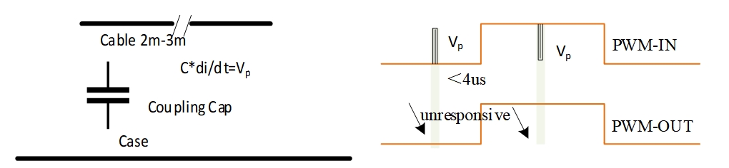
PWM cable coupling principle Gate driver process logic
Fig. 5 PWM Interference Principle
Prior to 2016, high-power systems universally used fiber optics for PWM transmission. Since 2018, large-power converters have adopted electrical cabling (15V) for PWM signals. As shown below, electromagnetic interference from PCS power devices coupling onto 2m-3m PWM cables can generate disruptive high/low-level pulses on the PWM signals. The ED-WP-CB series integrates minimum pulse suppression, filtering out sub-4μs pulses to significantly enhance the noise immunity and reliability of PCS converters.
4.Conclusion
The ED-WP-CB series enhances PCS converter performance through comprehensive three-level sequence management, built-in minimum dead-time protection, and pulse filtering capabilities.
5.Type Number

Driver Core
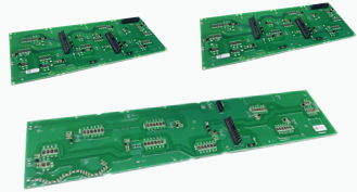
Adaptor Board
Fig. 6 ED-WP-CB Series Samples
| Power | Topology | Gate Driver | Matching |
| 1.25MW | 600A/1200V ANPC 3 in Parallel | ED-WP-CB1H15V-YA1A0D ED-WP-M4-3-60R12A2 A3ED130T23A1V-Y0004 | 1:1:1 |
| 1.75MW | 600A/1200V ANPC 4 in Parallel | ED-WP-CB1H15V-YA1A0D A2ED65T1456B1V-Y0010 A4ED130T23A1V-Y0004 | 1:2:1 |
| 2.5MW | ≥800A/1200V ANPC 4 in Parallel | ED-WP-CB1H15V-YA1A0D A2ED65T1456B1V-Y0010 A4ED130T23A1V-Y0004 | 1:2:1 |